
All Products
Contact Person :
Anna
Phone Number :
18620306819
WhatsApp :
+18620306819
High TG Ceramic two layer Qi Wireless Charger Circuit Board OEM ODM
| Place of Origin | Made in China |
|---|---|
| Brand Name | IBE |
| Certification | ISO 9001,ISO14001,UL |
| Model Number | IBE-9257 |
| Minimum Order Quantity | 1pc |
| Price | USD0.31 unit |
| Packaging Details | Vacuum bag+humidity indicator+carton |
| Delivery Time | 2-3 weeks |
| Payment Terms | T/T, L/C |
| Supply Ability | 100000sqm each month |
Product Details
| Material | FR4 Tg150 Shengyi | Colour | Black,green,yellow,blue |
|---|---|---|---|
| Copper Thickness | 1.5oz | Acceptable Standard | IPC-A-610F Class II Or III |
| Surface Finish | ENIG | Type | Custom Made |
| Product Name | Printed Circuit Board | Application | Bluetooth |
| Pcb Test | Electrical Test | Min.hole Size | 0.1mm |
| Silkscreen Color | White,yellow | Layers | 2 |
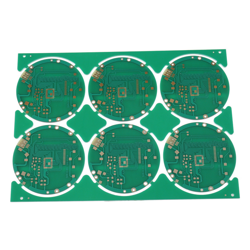
| Size | 60*60mm | Special | No X-out |
| High Light | High TG Ceramic two layer pcb,Qi Wireless Charger Circuit Board OEM,OEM ODM two layer pcb |
||
Product Description
2 layers PCB wireless charger pcb customized and layout with UL
| 1 | Material | PR4,Tg150 |
| 2 | Board Thickness | 1.0mm+/-10% |
| 3 | Surface Finish | ENIG |
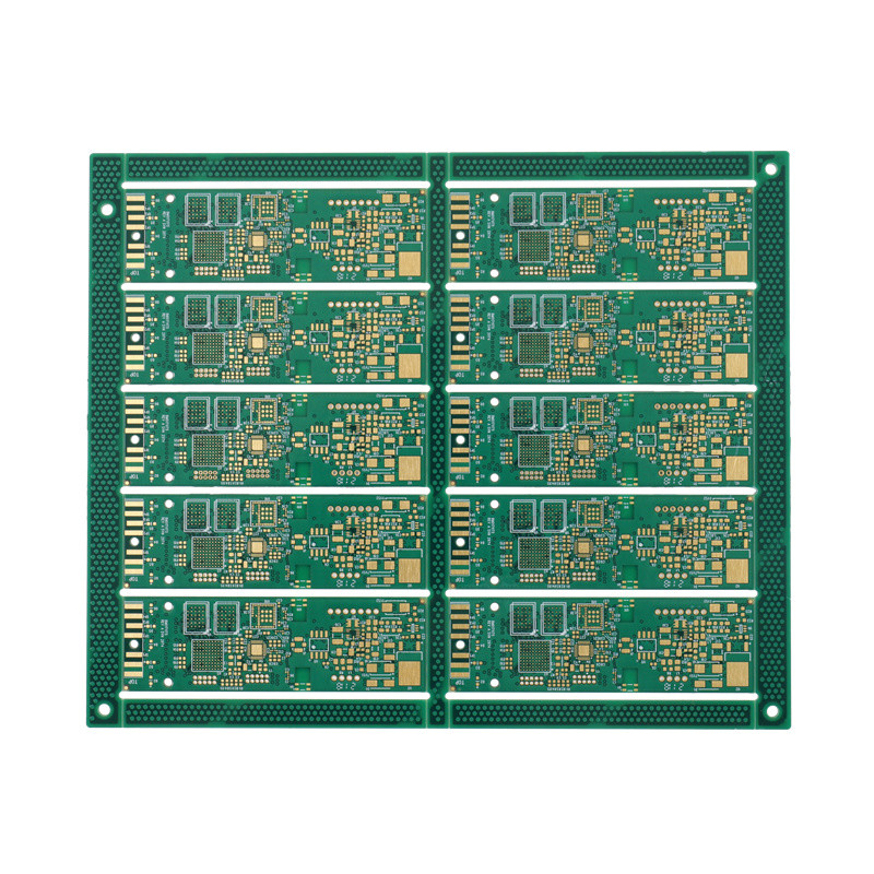
| 4 | PCB Panel Size | 130*190/6 |
| 5 | Layer | 2 |
| 6 | Min. Drill Hole Size | 0.1mm |
| 7 | PCB QC | Electrical test and automatically hole inspection; Appearance automatic detection |
| 8 | Application | wireless charger |
| 9 | Additional | half hole |
Since 2005, IBE provides Electronics Manufacturing Service (EMS) in China,US,Vietnam. As an ISO 9001 , UL,CSA and CCC certified manufacturer, We offers flexible, cost effective and high quality EMS solutions for printed circuit board assembly (PCBA) and complete product assembly through state of the art manufacturing technologies and production facilities.
With over 15 years manufacturing experience in electronics sectors, IBE is more than a reliable EMS provider for OEMs. Aiming at top notch manufacturing service and total customer satisfaction, we have maintained long term business partnerships with customers all around the world. Our products are mainly applied in the Consuming, Industrial, Automation, Automotive, Agriculture, Defense, Aerospace, Medical and Security markets.
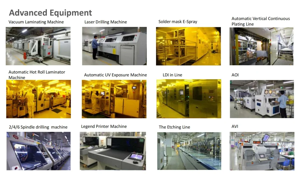
Our factory equipped with a variety of assembly technologies including Surface Mount Machine, PTH Insertion, COB, BGA, Flip, Wire Bonding, Box Build and Lead Free Soldering. Our production fact sheet is as following.
Our Advantages:
1, PCB Making (Rigid, Flexible,Rigid-Flexible,Aluminium, High TG,Ceramic), Component Sourcing, SMT&DIP, Free Program & Test, OEM/ODM Serivce
2, Factory Area:60000㎡ Shenzhen factory; two other factories in US and Vietnam
3, Certifcation:ATF 16949,ISO 13485,ISO 14001,ISO9001,UL(E326838),Disney FAMA, CE,FCC,ROHS,
Advanced Equipment
Recommended Products